CALL US
EMAIL US

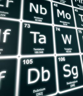
PVD Thin Film Coating Materials
Physical Vapour Deposition (PVD) Sputtering is a physical process where a target material used as the coating is bombarded with positively charged ionized gas molecules (typically Argon) in an inert gas chamber causing atoms to be “Sputtered” off into the plasma. These vaporised atoms are then deposited when they condense as a thin film on the substrate or wafer to be coated. This is also known as PVD Thin Film Coating.
PVD is specifically used in the manufacture of materials which require thin films for Mechanical, Optical, Chemical or Electronic functions. Electrical Conductivity, Hardness, Wear and Corrosion / Oxidation Resistance of a substrate will be significantly enhanced, improving its performance efficiency in areas of applications such as:
- Decorative
- Architectural
- Optoelectronics
- Semiconductor
- Data Storage
- Photovoltaics
- Tribology
PVD Sputtering Targets and Backing Plates are provided and available in a varied range of physical mechanical designs depending on customer specific PVD processes employed. Compositions and Purities of the Sputtering Targets are allowed for customisation to fulfil specific customer requirements.
PVD Target Processing Methods
- Machined Bar Stocks
- Vacuum Hot Pressing and Vacuum Sintering
- Cold / Hot Isostatic Pressing (CIP / HIP)
- Vacuum Induction Melting
- Melting and Casting
- Forging and Rolling
- C-Scan Ultrasonic Imagery
- Customized Backing Plates Machining from Bar Stocks
- Oxygen-Free High Conductivity Copper (OFHC)
- Molybdenum (Mo)
PVD Target Materials Design and Assembly Methods
- Planar Targets – Single Tile and Multiple Tiles
- Cylindrical Targets – Single Tile and Multiple Tiles
- Target Bonding Techniques
- Indium Metal Bonded Assembly – Target and Backing Plate
- Elastomer Bonded Assembly – Target and Backing Plate
- Nanofoil Bonded Assembly ~ Target and Backing Plate
Materials used for fabricating Sputtering Targets possess purities ranging from 99.5% – 99.999%:
- Pure Metals and Non-Metals (Ceramics)
- Carbides, Oxides, Borides and Nitrides
- Dual and Multiple Alloys
Typical PVD Sputtering Materials and Purities
Material | Composition | Purity % | Material | Composition | Purity % | Material | Composition | Purity % |
| Silver | Ag | 99.99 | Antimony | Sb | 99.9 | Hafnium | Hf | 99.9 |
| Aluminium | Al | 99.999 | Silicon | Si | 99.999 | Indium | In | 99.999 |
| Aluminium Copper | AlCu | 99.999 | Silicon Nitride | Si3N4 | 99.9 | Indium Tin Oxide | ITO | 99.99 |
| Aluminium Nitride | AlN | 99.0 | Silicon Dioxide | SiO2 | 99.995 | Iridium | Ir | 99.9 |
| Aluminium Oxide | Al2O3 | 99.99 | Tantalum | Ta | 99.95 | Lanthanum Trifluoride | LaF3 | 99.9 |
| Aluminium Silicon | AlSi | 99.999 | Tantalum Carbide | TaC | 99.5 | Manganese | Mg | 99.9 |
| Gold | Au | 99.99 | Terbium | Tb | 99.9 | Magnesium Oxide | MgO | 99.9 |
| Barium Oxide | BaO | 99.9 | Titanium | Ti | 99.995 | Manganese | Mn | 99.95 |
| Boron Nitride | BN | 99.99 | Titanium Carbide | TiC | 99.5 | Manganese Platinum | MnPt | 99.9 |
| Carbon | C | 99.999 | Titanium Dioxide | TiO2 | 99.9 | Molybdenum | Mo | 99.98 |
| Calcium Fluoride | CaF2 | 99.95 | Titanium Nitride | TiN | 99.5 | Molybdenum Disulfide | MoS2 | 99.0 |
| Cobalt | Co | 99.95 | Vanadium | V | 99.5 | Niobium | Nb | 99.95 |
| Copper Nickel | CoNi | 99.9 | Tungsten | W | 99.9 | Nickel | Ni | 99.999 |
| Chromium | Cr | 99.98 | Yttrium | Y | 99.9 | Nickel Chromium | NiCr | 99.95 |
| Copper | Cu | 99.999 | Zinc | Z | 99.99 | Nickel Iron | NiFe | 99.95 |
| Erbium | Er | 99.9 | Zinc Sulphide | ZnS | 99.9 | Nickel Vanadium | NiV | 99.95 |
| Iron | Fe | 99.95 | Zinc Selenide | ZnSe | 99.99 | Osmium | Os | 99.9 |
| Iron Manganese | FeMn | 99.9 | Zinc Oxide | ZnO | 99.99 | Lead | Pb | 99.99 |
| Germanium | Ge | 99.999 | Zinc Oxide Aluminium | ZnOAl | 99.90 | Palladium | Pd | 99.9 |
| Germanium Dioxide | GeO2 | 99.999 | Zirconium | Zr | 99.7 | Platinum | Pt | 99.99 |
| Rhenium | Re | 99.9 | Rhodium | Rh | 99.9 | Ruthenium | Ru | 99.95 |